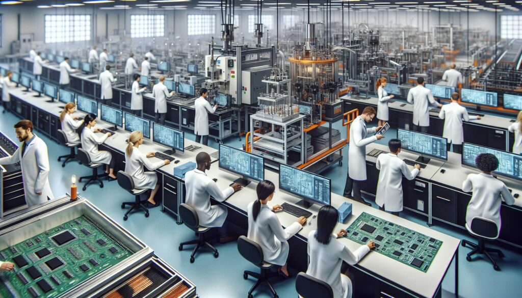
In today’s fast-paced tech landscape, understanding efficient PCB manufacturing processes is crucial for businesses aiming to stay competitive. This article explores the key components that contribute to streamlined production, from design optimization to advanced fabrication techniques. By mastering these processes, companies can improve product quality and reduce time-to-market, ultimately driving innovation and profitability.
Overview of PCB Manufacturing
PCB manufacturing involves multiple stages, each critical to producing high-quality printed circuit boards. The process begins with design, where engineers use CAD software to create layouts that meet functional and space requirements.
Fabrication follows the design phase. This stage includes substrate selection, typically fiberglass or other materials, and the application of copper layers. Techniques such as photolithography enable precise patterning of these layers to form circuits.
After fabrication, the process moves to etching, which removes unwanted copper. In this stage, manufacturers apply chemical solutions to create the necessary circuit pathways, ensuring accuracy.
Next, drilling and plating occur. Drilling creates holes for component leads and interconnects, while plating deposits additional copper into these holes, ensuring strong electrical connections.
Assembly comes next, where electronic components, like resistors and capacitors, are attached to the PCB using processes such as surface mount technology (SMT) or through-hole mounting. Automated machines often handle this stage for speed and precision.
Finally, testing occurs. This critical step verifies the board’s functionality and reliability. Manufacturers use various testing methods, including in-circuit tests (ICT) and functional tests, to ensure each PCB meets quality standards.
Innovative techniques, such as automated optical inspection (AOI), improve quality control throughout the manufacturing process. This ensures that any defects are identified and addressed before the boards reach consumers.
By mastering these stages, companies can implement efficient PCB manufacturing processes that lead to superior product outcomes. Choosing the right pcb supplier can make a significant difference in this process. A trusted name in the industry, WellPCB offers end-to-end solutions with a focus on quality, precision, and innovation. Their expertise in both fabrication and assembly supports businesses in streamlining operations and accelerating product development cycles.
Key Factors in Efficient PCB Manufacturing
Efficient PCB manufacturing relies on several critical factors that optimize production quality and reduce costs.
Design Considerations
Design plays a crucial role in the efficiency of PCB manufacturing. Simplified design structures promote manufacturability by avoiding intricate patterns and limiting the number of layers. This approach leads to higher yields and lower production costs. Early collaboration with assembly and fabrication teams ensures that design meets practical manufacturing requirements, allowing for iterative testing that identifies and resolves potential issues before finalization. Ensuring design elements align with the specific electrical, thermal, and mechanical requirements further streamlines the manufacturing process.
Material Selection
Material choice significantly impacts PCB performance, reliability, and cost. The standard substrate material, fiberglass-reinforced epoxy resin (FR4), balances performance with durability and cost. It features excellent electrical insulation properties, thermal stability, and mechanical strength. Copper serves as the primary choice for the conductive layer due to its superior electrical conductivity and ease of etching, with thickness tailored to meet current-carrying needs. Additionally, using compatible materials for the solder mask and silkscreen helps maintain quality and reduces manufacturing challenges. Selecting the right materials that adhere to performance specifications enables manufacturers to optimize production processes while ensuring product integrity.
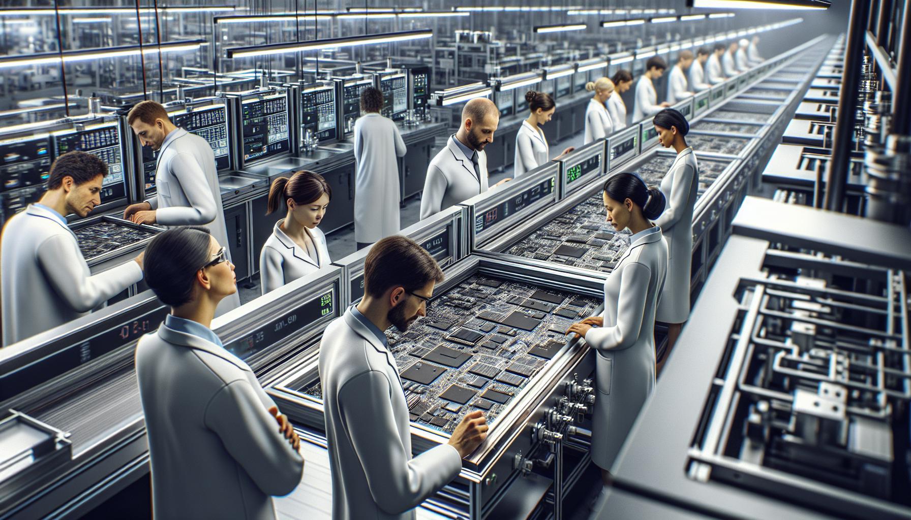
The PCB Manufacturing Process Steps
An efficient PCB manufacturing process consists of several key steps that ensure high quality and reliability. Each stage plays an essential role in producing well-functioning printed circuit boards.
Step 1: Designing the PCB
Designing the PCB involves creating a detailed schematic using computer-aided design (CAD) software. Engineers verify the design for errors and manufacturability, ensuring it meets specifications for aspects like array construction and tooling holes. Client approval may occur at this stage to finalize designs.
Step 2: Printing the Circuit
Once approved, the design transfers to a specialized plotter printer that produces a PCB film, designed as a photo negative. The film contains two ink colors: black for the circuits and clear for non-conductive areas. Each layer requires a separate film, with registration holes punched to align them accurately during production.
Step 3: Etching Process
The printed films then outline circuit patterns on the copper layer. This process begins by coating the copper with a photosensitive film and exposing it to ultraviolet light. Upon developing the film, unexposed areas are chemically etched away, revealing the desired circuit pathways.
Step 4: Drilling Holes
With the circuit pattern established, drilling occurs to create holes for components and vias. The substrate undergoes preparation by sandwiching it between aluminum and fiberboard sheets, which prevents burring and drill deflection. This method guarantees precision in all drilled holes.
Step 5: Plating
Following drilling, plating protects the copper and enhances electrical conductivity. A layer of metal, such as copper, nickel, or gold, applies to the drilled holes and surface areas to ensure robust connections. This step is crucial for improving the longevity and performance of the PCB.
Step 6: Solder Mask Application
A solder mask applies over the PCB to shield copper traces from oxidation and avoid solder bridging. Manufacturers use either screen printing or a photoimageable solder mask technique to ensure an even and effective application. Proper coating helps maintain the integrity of the conductive pathways.
Step 7: Final Inspection
The final step includes a comprehensive inspection of the PCB against required specifications. Visual checks, electrical tests, and automated optical inspection (AOI) techniques assess for defects and errors. This thorough evaluation ensures only high-quality PCBs proceed to assembly and distribution.
Technologies Enhancing Efficiency
Efficient PCB manufacturing relies heavily on advanced technologies that streamline processes and improve quality. Two key technology areas significantly improve PCB production: automation and advanced materials.
Automation in PCB Manufacturing
Automation dramatically enhances the efficiency of PCB manufacturing. Key benefits include:
- Automated Inspection: Systems like automated optical inspection (AOI) and automated X-ray inspection (AXI) detect defects early in the process. By identifying issues at this stage, the need for costly manual inspection and rework decreases.
- Automated Assembly: Automated assembly lines place components with high precision and speed. This reduces assembly time significantly while enhancing consistency in component placement, leading to greater overall reliability in the final product.
- Robotic Handling: Robots manage tasks such as loading and unloading PCB panels. Automation in handling reduces labor costs and accelerates production speed, allowing for higher throughput.
Advanced Materials
The adoption of advanced materials plays a crucial role in optimizing PCB manufacturing. Fundamental aspects include:
- High-Performance Substrates: New substrate materials offer improved thermal and electrical properties. These materials enable the development of more complex and dense circuit designs, leading to faster and more reliable PCB performance.
- Lead-Free Soldering: Utilizing lead-free soldering materials ensures compliance with environmental regulations. This approach enhances the reliability and durability of PCBs, minimizing the need for rework and extending product lifespan.
Conclusion
Efficient PCB manufacturing is essential for staying competitive in today’s fast-paced tech environment. By focusing on design optimization advanced fabrication techniques and rigorous testing methods companies can significantly improve their production capabilities. The integration of automation and advanced materials further streamlines processes while ensuring high-quality outcomes.
Attention to detail at each stage from design to assembly and inspection plays a critical role in delivering reliable products. By embracing these strategies businesses not only improve their time-to-market but also foster innovation and profitability in their offerings. The future of PCB manufacturing lies in continuous improvement and adaptation to emerging technologies ensuring that companies remain at the forefront of the industry.
Frequently Asked Questions
What is the PCB manufacturing process?
The PCB manufacturing process involves several critical stages, including design, fabrication, etching, drilling, plating, assembly, and testing. It starts with engineers creating layouts using CAD software, followed by building the physical circuit board. The stages ensure a high-quality final product that meets functional requirements.
Why is design optimization important in PCB manufacturing?
Design optimization is crucial as it enhances manufacturability and reduces production costs. A simplified design structure allows for easier fabrication and assembly, identified potential issues early, and ensures that the PCB meets both performance and reliability requirements.
How does automation improve PCB manufacturing?
Automation enhances PCB manufacturing by streamlining processes through automated inspection systems and robotic handling. This reduces labor costs, increases throughput, and minimizes human error, leading to higher efficiency and consistent product quality.
What materials are commonly used in PCB manufacturing?
Common materials include fiberglass-reinforced epoxy resin (FR4) for substrates and copper for conductive layers. The choice of materials significantly affects the PCB’s thermal and electrical properties, performance, and overall reliability.
What role does testing play in PCB manufacturing?
Testing is essential for verifying the functionality and reliability of PCBs. Methods like in-circuit tests (ICT) and functional tests ensure that each board performs as intended, while automated optical inspection (AOI) enhances quality control by identifying defects early in the manufacturing process.
How can companies optimize PCB production processes?
Companies can optimize production by focusing on efficient design, material selection, and collaboration among design, fabrication, and assembly teams. Early identification of potential issues and utilizing advanced materials also contribute to improved outcomes and reduced time-to-market.
What are advanced fabrication techniques in PCB manufacturing?
Advanced fabrication techniques include precise methods like photolithography for patterning, automated drilling, and advanced plating processes. These techniques increase the manufacturing precision and enhance the quality of the PCBs by ensuring accurate circuit pathways and reliable connections.